Search News
Industry Portal
Hot Articles
- How Factories Can Select Air Quality Controls for Dust, Fumes, and VOCsIndustrial air quality control for factories: learn how to select effective solutions for dust, fumes, and VOCs while improving safety, compliance, energy efficiency, and uptime.
- How to Size Industrial Gas Scrubbing Units for Acid Fumes and Variable AirflowsIndustrial gas scrubbing units: learn how to size acid-fume scrubbers for variable airflows, peak loads, chemical demand, pressure drop, and reliable compliance.
- How to Evaluate Industrial Air Quality Control Systems for Dust, Fumes, and VOCsIndustrial air quality control systems: learn how to evaluate dust, fumes, and VOC solutions by capture efficiency, compliance, maintenance, and lifecycle cost.
Popular Tags
What defines a stable semiconductor manufacturing environment
author
Time
Click Count
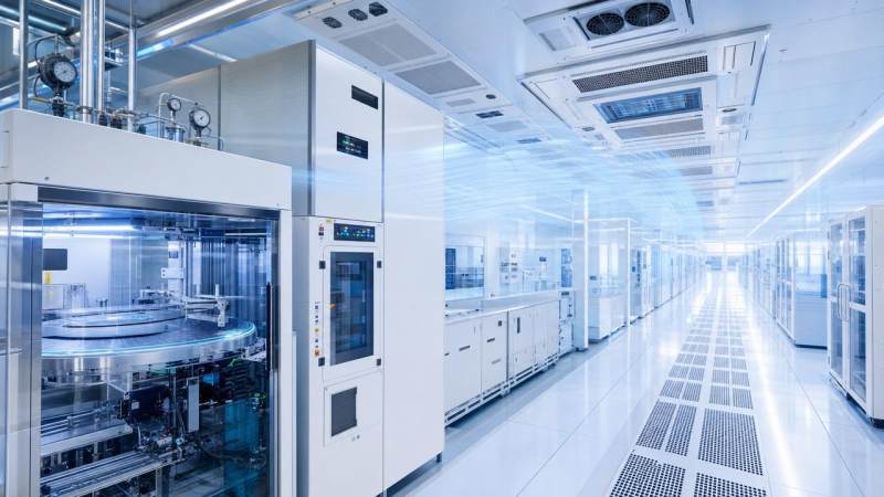
A stable semiconductor manufacturing environment is no longer judged by cleanliness alone. It is defined by how precisely a facility controls particles, temperature, humidity, airflow, vibration, and gas purity at the same time.
That shift matters because every environmental fluctuation can alter wafer yield, line stability, equipment uptime, and product consistency. In advanced fabs, tiny deviations often create expensive process drift long before alarms appear.
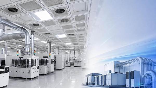
The modern semiconductor manufacturing environment has become a system-level discipline. It connects cleanroom engineering, precision HVAC, gas treatment, airflow design, and energy recovery into one continuous control strategy.
Why the semiconductor manufacturing environment is becoming harder to stabilize
Current industry signals show rising complexity across node scaling, material diversity, and sustainability compliance. As structures shrink, environmental tolerance windows become narrower, while utility efficiency targets become stricter.
Older assumptions no longer hold. A cleanroom that looked compliant on paper may still underperform if pressure cascades, return airflow, moisture control, or molecular contamination are not tightly coordinated.
This is why the semiconductor manufacturing environment is now treated as a yield tool, not only a building service. Environmental control directly shapes process capability and long-term operational resilience.
The strongest trend signals behind this change
- Higher wafer values increase the cost of contamination events.
- Advanced lithography and deposition demand tighter thermal stability.
- Moisture-sensitive chemicals require lower dew point control.
- ESG and zero-carbon goals push efficient ventilation and heat recovery.
- Global standards require more documented, auditable environmental performance.
What actually defines a stable semiconductor manufacturing environment
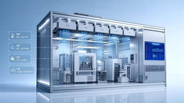
A stable semiconductor manufacturing environment is defined by consistency, not isolated peak performance. One perfect particle count reading means little if humidity swings, airflow turbulence, or trace gases disrupt the process later.
In practice, stability comes from maintaining controlled conditions across space, time, and process transitions. Startup, maintenance, shift changes, and seasonal weather all test real environmental robustness.
Core parameters that must remain synchronized
The main forces shaping next-generation environmental control
Several technical drivers explain why the semiconductor manufacturing environment now demands tighter and more integrated control than previous fab generations.
- Smaller features are less tolerant of particle intrusion and thermal drift.
- Wet and dry processes use chemistries sensitive to moisture and airborne molecules.
- High-density tool layouts complicate airflow paths and local heat loads.
- Energy intensity makes efficient CRAC, FFU, and ventilation design economically critical.
- Regulatory pressure increases the need for zero-emission gas treatment and documented compliance.
This is where integrated environmental intelligence becomes valuable. CECS closely tracks how molecular filtration, aerodynamic balance, desiccant dehumidification, and heat recovery are converging inside modern semiconductor infrastructure.
How control technologies support stability
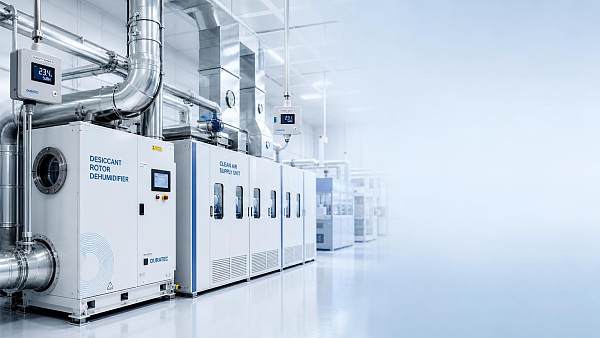
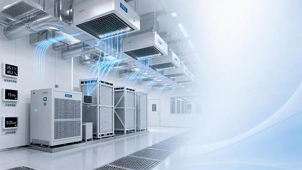
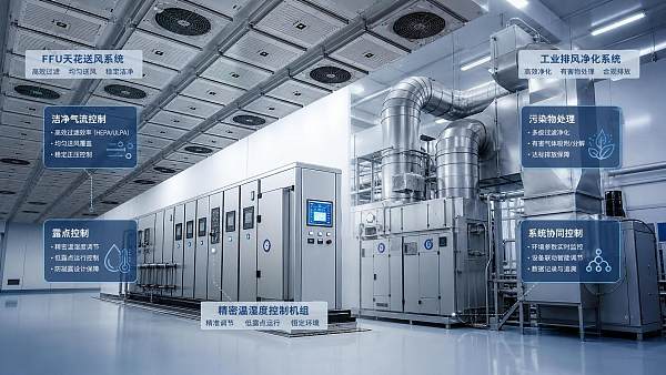
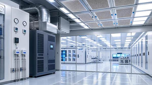
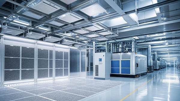
Precision CRAC units help hold narrow temperature and dew point bands. In moisture-sensitive lines, molecular sieve desiccant wheels can suppress dew point below -60°C for process protection.
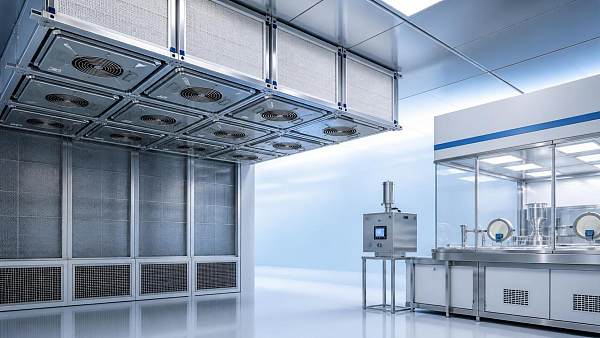
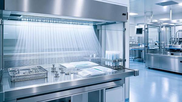
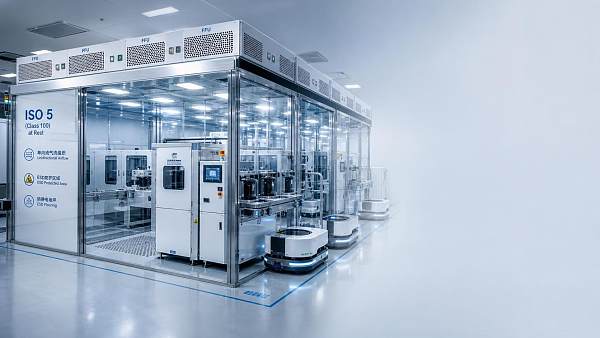
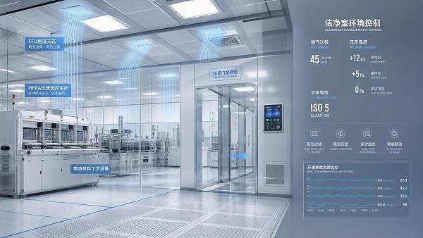
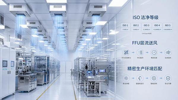
FFU arrays create the clean vertical laminar flow needed above wafer processing zones. Uniform airflow matters as much as filter efficiency because disturbed flow can redeposit particles onto critical surfaces.
Industrial scrubbers and gas treatment systems defend the semiconductor manufacturing environment from toxic exhaust interactions and external contamination risks. Stable internal conditions depend on safe, balanced exhaust management.
Energy recovery ventilation is also gaining value. It reduces HVAC burden while helping maintain controlled fresh air treatment, which matters as fabs pursue both uptime and decarbonization targets.
How instability affects different business and production links
An unstable semiconductor manufacturing environment does not create only one type of loss. Its impact spreads across process quality, utility cost, maintenance burden, compliance exposure, and expansion planning.
- Process stages face defect risk, recipe inconsistency, and higher rework rates.
- Facility operations face rising energy use, filter loading, and difficult balancing.
- Safety systems face pressure from corrosive, flammable, or reactive gas handling demands.
- Compliance performance suffers when monitoring data lacks traceability and stability evidence.
The most damaging issue is often hidden variability. Yield may decline gradually while the root cause remains distributed across airflow, micro-climate zones, and exhaust interactions rather than one obvious equipment failure.
What deserves the closest attention in a semiconductor manufacturing environment
The priority is not simply adding more equipment. It is identifying which environmental variables most strongly influence process sensitivity and then controlling them as one coordinated system.
Key focus points
- Map particle behavior, not just filter ratings.
- Track dew point at process-relevant locations, not only central plant outputs.
- Verify airflow uniformity above tools and within return paths.
- Separate clean zones by pressure strategy and contamination source profile.
- Evaluate molecular contamination alongside dust counts.
- Measure stability during transient events, including maintenance and restart periods.
- Compare energy efficiency with environmental precision, not as competing goals.
This integrated view reflects the broader CECS perspective. Environmental control has become an invisible moat for high-tech manufacturing, where filtration, thermodynamics, and compliance now reinforce each other.
Practical judgment framework for future decisions
When assessing a semiconductor manufacturing environment, a useful decision framework should connect risk, performance, and lifecycle economics rather than focusing on installation cost alone.
The next step is system thinking, not isolated upgrades
A stable semiconductor manufacturing environment is defined by coordinated precision. Particle control, thermal balance, humidity suppression, airflow uniformity, and gas treatment must work as one architecture.
The strongest future advantage will come from environmental systems that are both ultra-clean and energy-aware. That means combining FFU performance, precision CRAC control, compliant exhaust treatment, and smart ventilation logic.
For any facility review, start by identifying where environmental variation most directly threatens wafer yield. Then connect monitoring, airflow design, dew point control, and recovery efficiency into a measurable roadmap.
In this market, the semiconductor manufacturing environment is not a background condition. It is a strategic infrastructure layer that protects product quality, compliance confidence, and long-term manufacturing competitiveness.
Recommended News
 Aug 25, 2026How to Select Cleanroom Particle Control Equipment for ISO Class and Process RiskCleanroom particle control equipment selection starts with process risk, ISO class, and airflow design. Learn how to compare FFUs, filters, and monitoring for reliable performance.
 Aug 23, 2026How Laminar Airflow Supports Compliance and Contamination Control in Medical Device ManufacturingLaminar airflow for medical devices helps reduce contamination risk, support cleanroom compliance, and improve audit readiness—see how it protects product quality and manufacturing control.
 Aug 21, 2026How to Achieve Stable RH Precision Humidity Control in Cleanroom Production?Stable RH precision humidity control starts with process-based design. Learn how airflow, sensors, dehumidification, and recovery logic keep cleanroom production consistent and reliable.
 Aug 19, 2026What Drives Cleanroom Compliance Cost in Pharma and Semiconductor Projects?Cleanroom compliance cost in pharma and semiconductor projects depends on ISO class, airflow, humidity control, validation, and energy use. Learn what drives cost and how to avoid costly overdesign.
 Aug 11, 2026How to Select Precision Humidity Control for Cleanrooms and Micro-EnvironmentsPrecision humidity control for cleanrooms starts with process needs. Learn how to compare dew point targets, airflow, controls, and energy tradeoffs for reliable, high-yield micro-environments.
 Aug 05, 2026How Cleanroom Environmental Control Automation Improves Compliance and StabilityCleanroom environmental control automation improves compliance, stability, and audit readiness through faster response, traceable control logic, and consistent environmental performance.
 Aug 04, 2026How Smart Cleanroom Thermal Control Improves Stability in FFU-Based Micro-EnvironmentsSmart cleanroom thermal control improves FFU-based micro-environment stability by aligning temperature, humidity, pressure, and airflow—learn what to evaluate before performance drifts.
 Aug 03, 2026Semiconductor Cleanroom Standards Explained: ISO Classes, Air Changes, and ESD ControlsCleanroom standards for semiconductor industry explained: understand ISO classes, air changes, and ESD controls to improve yield, reduce contamination risk, and choose smarter fab environments.
 Jul 30, 2026How to Choose Environmental Control Solutions for High-Tech Manufacturing FacilitiesHigh-tech manufacturing environment solutions guide: learn how to evaluate cleanroom airflow, dew point control, exhaust treatment, and compliance to protect yield and cut lifecycle risk.
 Jul 29, 2026How to Design Ventilation for Precision Manufacturing to Control Particles and HeatPrecision manufacturing ventilation design guide: learn how to control particles, heat, airflow, filtration, and pressure for cleaner production, higher yield, and more reliable operations.
 Jul 26, 2026ISO 5 Semiconductor Cleanroom Solutions: Key Design Criteria for Process StabilityISO 5 semiconductor cleanroom solutions focus on process stability, airflow uniformity, pressure control, and thermal consistency to protect yield and improve fab performance.
 Jul 24, 2026Cleanroom Standards Compliance: Key Requirements and Audit Readiness ChecklistCleanroom standards compliance starts with real control, not paperwork. Explore key ISO requirements, common audit gaps, and a practical checklist to improve readiness.
 Jul 20, 2026How to Evaluate a Semiconductor Cleanroom Solutions Supplier for Fab ProjectsSemiconductor cleanroom solutions supplier selection can make or break fab performance. Learn how to compare engineering depth, compliance, delivery, and lifecycle value.
 Jul 15, 2026Dust-Free Manufacturing: Key Process Controls for Cleaner Production LinesDust-free manufacturing starts with tighter control of airflow, humidity, filtration, and gas capture. Discover how cleaner production lines improve yield, safety, compliance, and energy performance.
 Jul 13, 2026How Semiconductor Environmental Control AMC Reduction Prevents Yield LossSemiconductor environmental control AMC reduction is essential to prevent yield loss. Learn how airflow, humidity, filtration, and gas treatment protect fabs and improve process stability.
 Jul 12, 2026How to Choose Semiconductor Cleanroom Solutions for EUV Lithography LinesSemiconductor cleanroom solutions for EUV require more than ISO class compliance. Learn how to compare airflow, AMC, thermal stability, vibration, and lifecycle cost for better yield.
 Jul 11, 2026Cleanroom Design Criteria Explained: Air Changes, Pressure Cascade, and ISO ClassCleanroom design criteria explained: learn how air changes, pressure cascade, and ISO Class work together to improve contamination control, compliance, and process stability.
 Jul 09, 2026Semiconductor Facility Ventilation Standards: Pressure Cascade, Air Changes, and ComplianceSemiconductor facility ventilation explained: pressure cascade, air changes, and compliance essentials to protect yield, control contamination, and reduce hidden operational risk.
 Jul 09, 2026Clean Environment Control Solutions for Dust, Humidity, and ESD in Sensitive ProductionClean environment control solutions for dust, humidity, and ESD help sensitive production improve yield, ensure compliance, cut energy waste, and reduce costly rework.
 Jul 08, 2026Cleanroom Standards ISO Class Explained: How to Match Class Levels to ProductionCleanroom standards ISO class explained clearly: learn how to match class levels to production needs, reduce contamination risk, control costs, and choose smarter cleanroom strategies.
 Jul 08, 2026How Electronics Cleanroom Air Showers Reduce Particle Transfer at Entry PointsElectronics cleanroom air showers reduce particle transfer at entry points, protect sensitive processes, and support better yield, cleaner airflow, and more reliable contamination control.
![]() Jul 07, 2026Cleanroom Certification USA: ISO Classes, Testing Steps, and Common Compliance GapsCleanroom certification USA explained: compare ISO classes, understand key testing steps, and spot common compliance gaps before they trigger audit issues, downtime, or product risk.
Jul 07, 2026Cleanroom Certification USA: ISO Classes, Testing Steps, and Common Compliance GapsCleanroom certification USA explained: compare ISO classes, understand key testing steps, and spot common compliance gaps before they trigger audit issues, downtime, or product risk. Jul 06, 2026What Is Semiconductor Clean Air and Why Does It Matter in Contamination Control?Semiconductor clean air is vital to contamination control, protecting yield, tool stability, and process consistency. Learn why it matters in modern fabs.
 Jul 05, 2026Cleanroom Airflow Control Systems Explained: How to Balance Pressure, Air Changes, and StabilityCleanroom airflow control systems explained: learn how to balance pressure, air changes, and stability to improve contamination control, cut energy waste, and protect production yield.