Search News
Industry Portal
Hot Articles
- How Factories Can Select Air Quality Controls for Dust, Fumes, and VOCsIndustrial air quality control for factories: learn how to select effective solutions for dust, fumes, and VOCs while improving safety, compliance, energy efficiency, and uptime.
- How to Size Industrial Gas Scrubbing Units for Acid Fumes and Variable AirflowsIndustrial gas scrubbing units: learn how to size acid-fume scrubbers for variable airflows, peak loads, chemical demand, pressure drop, and reliable compliance.
- How to Evaluate Industrial Air Quality Control Systems for Dust, Fumes, and VOCsIndustrial air quality control systems: learn how to evaluate dust, fumes, and VOC solutions by capture efficiency, compliance, maintenance, and lifecycle cost.
Popular Tags
How semiconductor manufacturing HVAC affects wafer yield
author
Time
Click Count
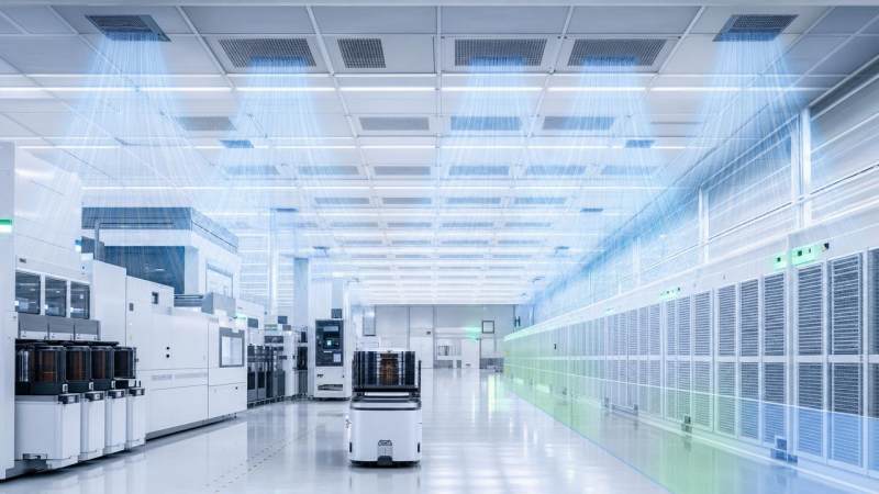
In semiconductor fabs, HVAC is far more than a utility system—it is a decisive factor in contamination control, temperature stability, humidity precision, and ultimately wafer yield. Understanding how semiconductor manufacturing HVAC shapes process consistency helps reduce defects, protect capital-intensive production, and strengthen competitiveness where microscopic environmental drift can trigger major financial loss.
Why a checklist approach matters for semiconductor manufacturing HVAC
Semiconductor production links lithography, etch, deposition, cleaning, and packaging through tightly controlled environmental conditions. HVAC failures rarely stay isolated. They spread through airflow, moisture, static, and pressure imbalance.
A checklist prevents teams from treating HVAC as a background asset. In fabs, semiconductor manufacturing HVAC directly affects particles, chemical stability, tool uptime, operator safety, and cleanroom energy intensity.
This matters across the broader industrial landscape too. Lessons from high-spec cleanrooms increasingly influence battery plants, precision electronics, pharmaceutical spaces, and zero-carbon facilities seeking tighter environmental control.
Core checklist: what to verify first
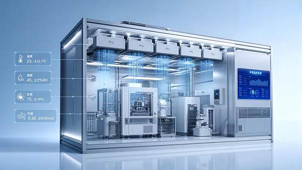
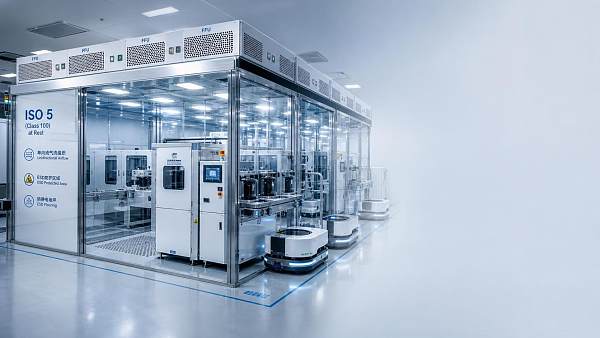
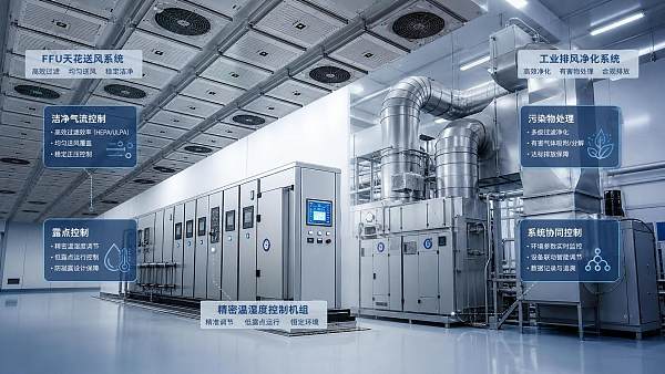
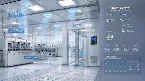
- Confirm particle targets by process zone, then align FFU coverage, HEPA or ULPA grade, and laminar flow velocity with actual tool sensitivity.
- Stabilize temperature within process-specific limits, because even slight drift can distort overlay accuracy, resist behavior, and metrology repeatability.
- Control relative humidity and dew point tightly to reduce electrostatic discharge, moisture absorption, corrosion risk, and material instability.
- Maintain room pressure cascades between corridors, ballrooms, sub-fabs, and chemical rooms to stop backflow contamination and fugitive gas migration.
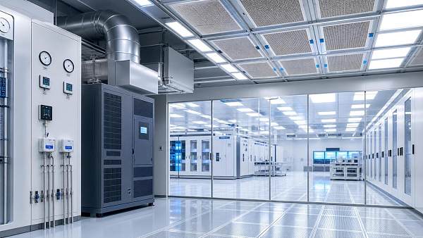
- Measure airflow uniformity above tools, not only at air handlers, because local turbulence can raise defect density despite acceptable central readings.
- Review make-up air treatment, especially filtration, dehumidification, and reheating stages, to avoid outdoor weather swings reaching the clean space.
- Inspect return air paths under raised floors or ceiling plenums, since blocked recirculation often causes hot spots and unstable contamination patterns.
- Check chemical exhaust coordination with supply air volumes so hazardous vapors are captured without upsetting pressure balance or thermal stability.
- Validate sensor placement and calibration frequency, because misplaced probes can hide true process conditions near wafer handling positions.
- Track energy performance together with yield indicators, ensuring efficiency projects never weaken the environmental precision required by the fab.
How semiconductor manufacturing HVAC affects wafer yield at process level
Particle control and defect prevention
A single airborne particle can shadow a pattern, scratch a surface, or interfere with deposition. That is why semiconductor manufacturing HVAC starts with disciplined filtration and airflow architecture.
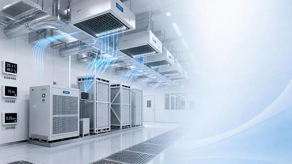
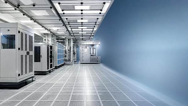
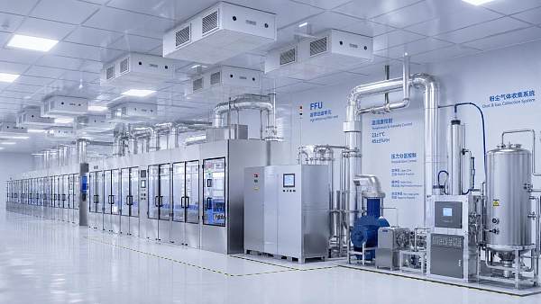
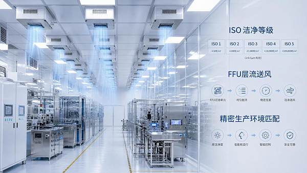
FFUs, ceiling grids, and pressure zoning must support stable downward laminar flow. If velocity is uneven, particles can circulate around tool load ports and settle on wafers.
Temperature stability and overlay accuracy
Lithography is especially sensitive to thermal change. Small temperature variation can alter wafer expansion, lens performance, and resist response, reducing alignment precision between layers.
Beyond lithography, etch rates, CMP behavior, and inspection repeatability also depend on stable ambient conditions. Effective semiconductor manufacturing HVAC minimizes these hidden process shifts.
Humidity control and electrostatic risk
Low humidity can increase electrostatic discharge, which threatens sensitive devices and wafer handling systems. High humidity can introduce condensation risk, chemical instability, and corrosion.
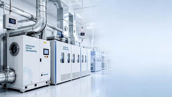
Advanced fabs often need very low dew points in selected zones. Desiccant systems, precision CRAC units, and fast control loops become essential, not optional.
Pressure control and chemical safety
Sub-fabs, wet benches, gas cabinets, and solvent areas require coordinated airflow. Poor pressure relationships can pull corrosive gases into clean spaces or interfere with process exhaust capture.
Yield damage may then appear indirect. Corrosion on tools, unstable sensors, and airborne molecular contamination can degrade process windows before alarms clearly identify the source.
Application scenarios that need different HVAC priorities
Front-end wafer fabrication
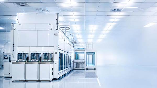
Front-end fabs demand the strictest environmental discipline. Here, semiconductor manufacturing HVAC must protect nanometer-scale features from particles, thermal drift, and airborne chemicals.
The focus should stay on ULPA-level filtration, airflow uniformity above critical tools, robust dew point suppression, and real-time differential pressure monitoring across process bays.
Back-end packaging and testing
Packaging areas may not require the same cleanliness class as advanced lithography zones, but temperature and humidity still shape bond quality, material curing, and ESD control.
A right-sized strategy improves cost control. The objective is not overdesign everywhere, but targeted environmental precision where defects or rework are most expensive.
Retrofit and expansion projects
When production expands, existing systems often become the hidden bottleneck. Added tools can disrupt return air patterns, cooling loads, and pressure cascades.
In retrofit settings, semiconductor manufacturing HVAC should be reviewed through airflow simulation, phased balancing, and contamination mapping before full ramp-up begins.
Commonly overlooked risks
Ignoring local airflow near tools. Central system performance can appear acceptable while wafer loading zones experience micro-turbulence and elevated particle deposition.
Assuming cleanroom class guarantees yield. ISO class compliance does not automatically control airborne molecular contamination, thermal gradients, or pressure instability.
Separating HVAC data from yield data. Without cross-analysis, facilities teams may miss recurring links between defect excursions and environmental drift.
Underestimating maintenance timing. Filter loading, damper wear, sensor drift, and coil fouling gradually reduce precision before they trigger obvious failures.
Chasing energy savings blindly. Lower airflow or relaxed setpoints can reduce utility cost but damage wafer yield, making the apparent savings financially negative.
Practical execution recommendations
- Map every critical process step to environmental limits, then rank zones by defect sensitivity rather than by building layout alone.
- Install monitoring points near wafers, FOUP paths, and tool interfaces, not only in main ducts or remote wall positions.
- Compare HVAC excursions with SPC, scrap events, and maintenance logs to identify repeatable yield-impact mechanisms.
- Use predictive maintenance for filters, fans, coils, and sensors to prevent gradual performance decay in cleanroom control.
- Model airflow and heat load before adding equipment, changing partitions, or revising exhaust volumes during capacity expansion.
- Balance compliance, cleanliness, and energy recovery so sustainability measures reinforce, rather than weaken, process reliability.
Conclusion and next steps
The impact of semiconductor manufacturing HVAC on wafer yield is direct, measurable, and often underestimated. Clean air delivery, thermal consistency, humidity precision, and pressure control all shape process capability.
A practical next step is to audit the fab by zone, compare environmental trends with defect data, and prioritize the highest-value corrections first. In advanced manufacturing, the invisible environment is often the real process moat.
Recommended News
 Aug 25, 2026How to Select Cleanroom Particle Control Equipment for ISO Class and Process RiskCleanroom particle control equipment selection starts with process risk, ISO class, and airflow design. Learn how to compare FFUs, filters, and monitoring for reliable performance.
 Aug 23, 2026How Laminar Airflow Supports Compliance and Contamination Control in Medical Device ManufacturingLaminar airflow for medical devices helps reduce contamination risk, support cleanroom compliance, and improve audit readiness—see how it protects product quality and manufacturing control.
 Aug 21, 2026How to Achieve Stable RH Precision Humidity Control in Cleanroom Production?Stable RH precision humidity control starts with process-based design. Learn how airflow, sensors, dehumidification, and recovery logic keep cleanroom production consistent and reliable.
 Aug 19, 2026What Drives Cleanroom Compliance Cost in Pharma and Semiconductor Projects?Cleanroom compliance cost in pharma and semiconductor projects depends on ISO class, airflow, humidity control, validation, and energy use. Learn what drives cost and how to avoid costly overdesign.
 Aug 11, 2026How to Select Precision Humidity Control for Cleanrooms and Micro-EnvironmentsPrecision humidity control for cleanrooms starts with process needs. Learn how to compare dew point targets, airflow, controls, and energy tradeoffs for reliable, high-yield micro-environments.
 Aug 05, 2026How Cleanroom Environmental Control Automation Improves Compliance and StabilityCleanroom environmental control automation improves compliance, stability, and audit readiness through faster response, traceable control logic, and consistent environmental performance.
 Aug 04, 2026How Smart Cleanroom Thermal Control Improves Stability in FFU-Based Micro-EnvironmentsSmart cleanroom thermal control improves FFU-based micro-environment stability by aligning temperature, humidity, pressure, and airflow—learn what to evaluate before performance drifts.
 Aug 03, 2026Semiconductor Cleanroom Standards Explained: ISO Classes, Air Changes, and ESD ControlsCleanroom standards for semiconductor industry explained: understand ISO classes, air changes, and ESD controls to improve yield, reduce contamination risk, and choose smarter fab environments.
 Jul 30, 2026How to Choose Environmental Control Solutions for High-Tech Manufacturing FacilitiesHigh-tech manufacturing environment solutions guide: learn how to evaluate cleanroom airflow, dew point control, exhaust treatment, and compliance to protect yield and cut lifecycle risk.
 Jul 29, 2026How to Design Ventilation for Precision Manufacturing to Control Particles and HeatPrecision manufacturing ventilation design guide: learn how to control particles, heat, airflow, filtration, and pressure for cleaner production, higher yield, and more reliable operations.
 Jul 26, 2026ISO 5 Semiconductor Cleanroom Solutions: Key Design Criteria for Process StabilityISO 5 semiconductor cleanroom solutions focus on process stability, airflow uniformity, pressure control, and thermal consistency to protect yield and improve fab performance.
 Jul 24, 2026Cleanroom Standards Compliance: Key Requirements and Audit Readiness ChecklistCleanroom standards compliance starts with real control, not paperwork. Explore key ISO requirements, common audit gaps, and a practical checklist to improve readiness.
 Jul 20, 2026How to Evaluate a Semiconductor Cleanroom Solutions Supplier for Fab ProjectsSemiconductor cleanroom solutions supplier selection can make or break fab performance. Learn how to compare engineering depth, compliance, delivery, and lifecycle value.
 Jul 15, 2026Dust-Free Manufacturing: Key Process Controls for Cleaner Production LinesDust-free manufacturing starts with tighter control of airflow, humidity, filtration, and gas capture. Discover how cleaner production lines improve yield, safety, compliance, and energy performance.
 Jul 13, 2026How Semiconductor Environmental Control AMC Reduction Prevents Yield LossSemiconductor environmental control AMC reduction is essential to prevent yield loss. Learn how airflow, humidity, filtration, and gas treatment protect fabs and improve process stability.
 Jul 12, 2026How to Choose Semiconductor Cleanroom Solutions for EUV Lithography LinesSemiconductor cleanroom solutions for EUV require more than ISO class compliance. Learn how to compare airflow, AMC, thermal stability, vibration, and lifecycle cost for better yield.
 Jul 11, 2026Cleanroom Design Criteria Explained: Air Changes, Pressure Cascade, and ISO ClassCleanroom design criteria explained: learn how air changes, pressure cascade, and ISO Class work together to improve contamination control, compliance, and process stability.
 Jul 09, 2026Semiconductor Facility Ventilation Standards: Pressure Cascade, Air Changes, and ComplianceSemiconductor facility ventilation explained: pressure cascade, air changes, and compliance essentials to protect yield, control contamination, and reduce hidden operational risk.
 Jul 09, 2026Clean Environment Control Solutions for Dust, Humidity, and ESD in Sensitive ProductionClean environment control solutions for dust, humidity, and ESD help sensitive production improve yield, ensure compliance, cut energy waste, and reduce costly rework.
 Jul 08, 2026Cleanroom Standards ISO Class Explained: How to Match Class Levels to ProductionCleanroom standards ISO class explained clearly: learn how to match class levels to production needs, reduce contamination risk, control costs, and choose smarter cleanroom strategies.
 Jul 08, 2026How Electronics Cleanroom Air Showers Reduce Particle Transfer at Entry PointsElectronics cleanroom air showers reduce particle transfer at entry points, protect sensitive processes, and support better yield, cleaner airflow, and more reliable contamination control.
![]() Jul 07, 2026Cleanroom Certification USA: ISO Classes, Testing Steps, and Common Compliance GapsCleanroom certification USA explained: compare ISO classes, understand key testing steps, and spot common compliance gaps before they trigger audit issues, downtime, or product risk.
Jul 07, 2026Cleanroom Certification USA: ISO Classes, Testing Steps, and Common Compliance GapsCleanroom certification USA explained: compare ISO classes, understand key testing steps, and spot common compliance gaps before they trigger audit issues, downtime, or product risk. Jul 06, 2026What Is Semiconductor Clean Air and Why Does It Matter in Contamination Control?Semiconductor clean air is vital to contamination control, protecting yield, tool stability, and process consistency. Learn why it matters in modern fabs.
 Jul 05, 2026Cleanroom Airflow Control Systems Explained: How to Balance Pressure, Air Changes, and StabilityCleanroom airflow control systems explained: learn how to balance pressure, air changes, and stability to improve contamination control, cut energy waste, and protect production yield.